
The ESP32's Wi-Fi and Bluetooth radios live or die by the RF layout, and the microstrip traces carrying 2.4 GHz signals to the antenna are the most sensitive copper on the board. A solid ground plane beneath those traces, forming a proper microstrip structure, is what keeps the signal intact instead of radiating into the board or picking up noise. Getting the ground plane right is RF layout fundamentals applied to a maker-friendly chip.
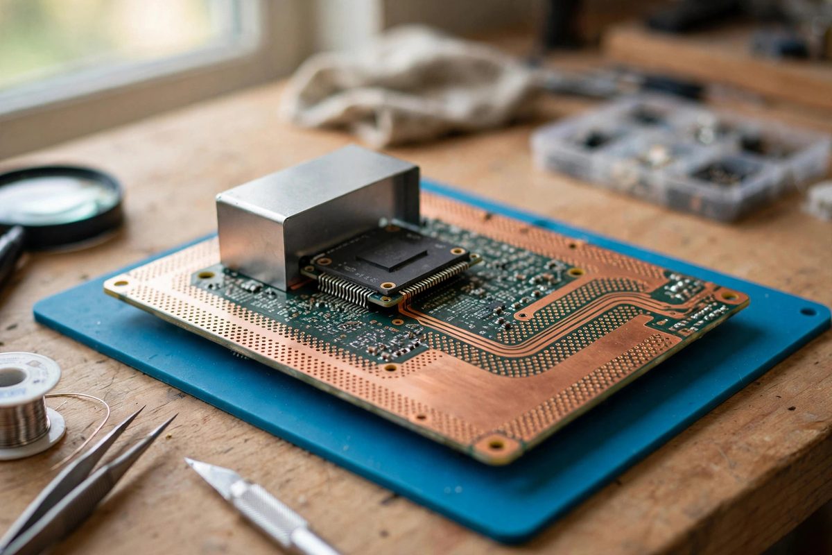
How the Microstrip and Ground Plane Work Together
A microstrip is a trace over a ground plane, separated by the PCB dielectric; the electromagnetic field of the signal lives mostly in the dielectric between the trace and the plane. The ground plane provides the return current path directly beneath the trace, which minimizes the loop area and therefore the radiation and susceptibility. The trace width, dielectric thickness, and dielectric constant together set the characteristic impedance, which for ESP32 RF work should be 50 ohms to match the chip's output and the antenna. Without the ground plane, the trace is just a wire with uncontrolled impedance; reflections at every discontinuity rob power and distort the signal. The plane is not optional copper; it is half the transmission line.
Keeping the Ground Plane Solid
The ground plane under RF traces must be continuous: no slots, no splits, no voids beneath the microstrip. A slot in the plane forces the return current to detour around it, which increases inductance, radiates energy, and changes the impedance; at 2.4 GHz, even a small slot is a significant defect. Route no signals through the RF ground region on any layer; keep the area under and around the antenna feed a dedicated, unbroken ground. If the board needs a keepout under the antenna itself, follow the module or chip manufacturer's layout guidance exactly, since the antenna's tuning assumes a specific ground geometry. Stitch the ground planes of multiple layers together with vias around the RF section to keep them at the same potential; a floating plane section resonates and causes trouble.
Trace Geometry for 50 Ohms
Calculate the microstrip width for 50 ohms using the board stackup: dielectric thickness and dielectric constant from the PCB fabricator. For common two-layer boards with standard thickness, the 50-ohm trace is relatively wide; for four-layer boards with thin prepreg, it is narrower. Use a microstrip calculator with the actual stackup numbers, not a generic table, since the wrong width means the wrong impedance. Keep the RF trace as short as possible and route it straight; every bend is a discontinuity, and while gentle bends are acceptable, sharp corners and unnecessary length add loss. Do not place components or test points on the RF trace; the feed should run uninterrupted from the chip's RF pin to the antenna or connector.
Shielding Against Noise and Interference
The ground plane shields the microstrip from noise below, but the trace's top side is exposed. Keep noisy circuits, switching regulators, high-speed digital lines, and especially the ESP32's own digital switching noise away from the RF section; physical separation is the first defense. A grounded metal shield can over the RF section provides excellent isolation in noisy designs, but it changes the electromagnetic environment and must be accounted for in the antenna area; never cover the antenna itself with a shield. Filter the power supply to the RF section with proper decoupling right at the chip; supply noise modulates the radio directly. Remember that shielding works both ways: a well-shielded RF section also keeps the 2.4 GHz energy from desensitizing nearby sensitive circuits.
Verification and Debugging
Verify the RF layout by testing, since few makers have network analyzers. The practical tests are range, throughput, and packet loss compared against a reference design; a board with a broken ground plane shows markedly worse range. If performance is poor, inspect the layout first: look for plane slots under the RF trace, wrong trace width, or components crowding the feed. Check that the ground vias actually connect the planes; an unconnected via is just a hole. Compare against the manufacturer's reference layout, which is proven; deviations from it need justification. RF layout is one of the few areas where copying the reference exactly is the professional move, not a shortcut.
The ESP32's microstrip needs its ground plane the way a wire needs its insulation: keep the plane solid and continuous, size the trace for 50 ohms on your actual stackup, isolate the RF section from noise, and verify with range testing. The radio can only be as good as the copper feeding it.
Related Guides
- RF Ground Plane Isolation on Directional Wi-Fi Boards: A directional Wi-Fi board, a patch antenna or a small array feeding an ESP32 bridge, lives or dies by its RF ground plane. The ground plane is part
- AP Station Isolation Protocols for ESP32 Mesh: ESP32 mesh networks, where each node relays for the others to extend coverage, often include an access point interface so phones, laptops, or sensors
- NAT Routing Throughput Limits on ESP32 Bridges: Using an ESP32 as a Wi-Fi bridge, relaying traffic between networks with network address translation, is a tempting trick: the chip has Wi-Fi, it
- High-Gain Directional Wi-Fi Bridge Antennas: When an ESP32 project needs to reach across a yard, between buildings, or to the far corner of a property, the stock antenna gives up long before the