
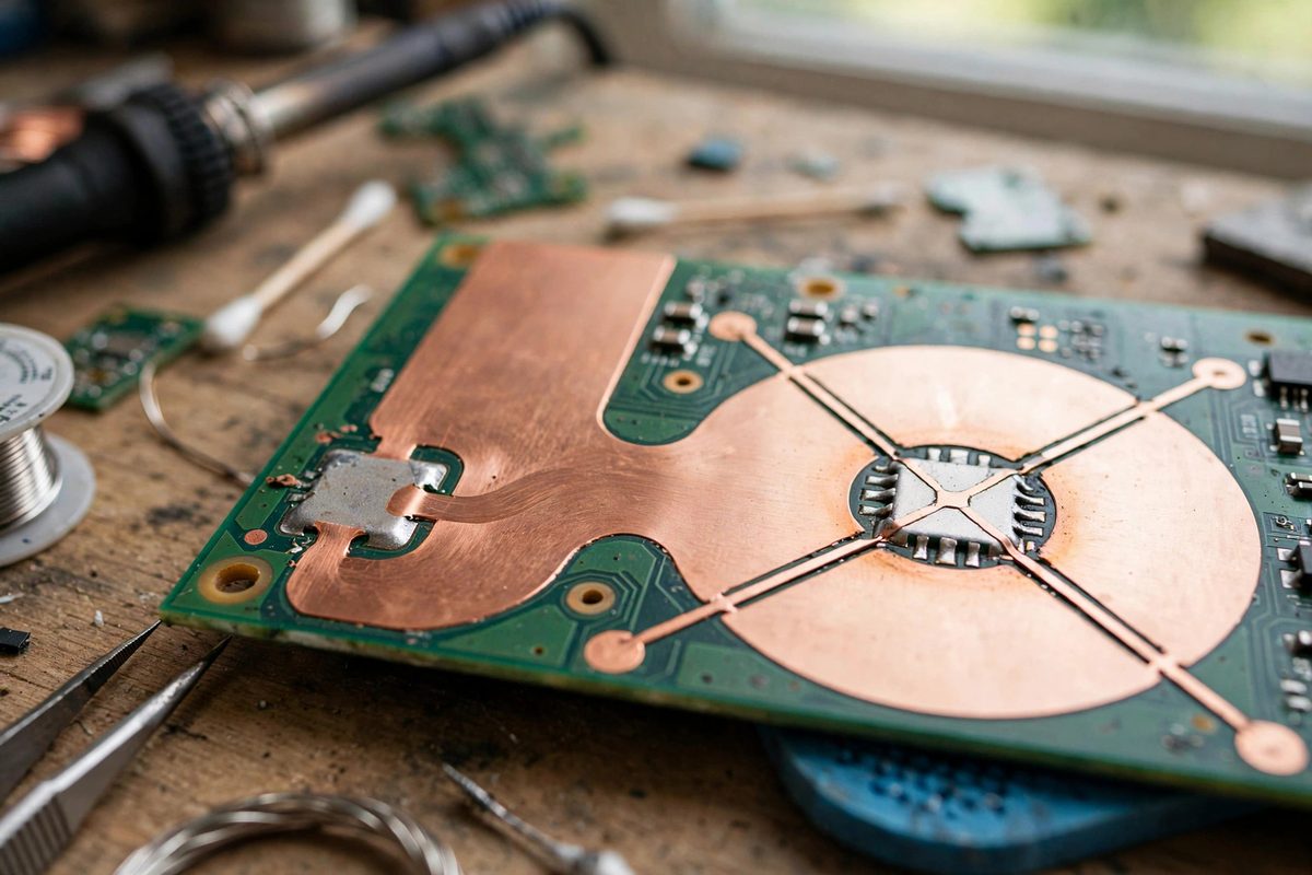
A pad connected directly to a large copper pour acts as a heatsink during soldering: the pour wicks heat away and the joint never flows properly. Thermal reliefs, the small spokes connecting the pad to the pour, limit that heat loss. On fine pitch pads, where the geometry is tiny and the spokes are fragile, the spoke angle and width determine whether the joint solders well and whether the pad survives assembly.
What Thermal Reliefs Do
During soldering, the iron or the reflow oven must bring the pad and the component lead to soldering temperature together. A pad fused solidly to a ground plane pours heat into the plane as fast as the iron supplies it; the solder melts sluggishly, flows poorly, and forms a weak, grainy joint, or the assembler overheats the component trying to compensate. Thermal relief spokes narrow the copper connection to the pour, throttling the heat flow so the pad reaches temperature quickly. The trade-off is electrical and mechanical: the spokes add a small resistance and inductance, and they are the pad's only mechanical attachment to the board. On fine pitch parts, where pads are small and close together, getting this balance right matters more than on chunky through-hole parts.
Spoke Angle and Heat Flow
The spokes typically connect at 45-degree angles to the pad, four spokes for a round pad, two or four for a rectangular SMD pad depending on the pour geometry. The angle matters because it sets the spoke length for a given air gap: 45-degree spokes are longer than radial spokes would be, and longer spokes throttle heat better. On fine pitch pads, the spokes must also fit between adjacent pads without violating clearance; the 45-degree angle naturally routes the spokes into the diagonal spaces between neighboring pads, which is why it is the standard. Avoid spoke angles that aim directly at an adjacent pad; the spoke plus the required clearance can bridge the gap. In the PCB editor, the thermal relief settings control the spoke width and the air gap; set them for the fine pitch reality, not the default, which is usually sized for larger parts.
Sizing Spokes for Fine Pitch
Spoke width is the main tuning knob. Wider spokes conduct more heat, soldering worse but surviving better mechanically and carrying more current; narrower spokes solder beautifully but are fragile and resistive. For fine pitch signal pads, favor narrower spokes, since the currents are small and solderability is the priority; the pad's mechanical strength comes mostly from the solder fillet anyway. For fine pitch power pads, the tension is real: the pad needs current capacity but also must solder. A common compromise uses the full allowed spoke width on power pads and accepts slightly more soldering heat, while keeping signal pads delicate. Check the spoke width against the fab's minimum copper width; spokes drawn too narrow may not etch reliably, producing broken reliefs that isolate the pad entirely.
Solderability Versus Tombstoning
Uneven thermal reliefs cause tombstoning on small chip components: if one pad of a resistor connects to a pour with weak reliefs while the other connects to a thin trace, the well-relieved pad heats faster, its solder melts first, and surface tension stands the component on end. The fix is thermal symmetry: give both pads of each component equivalent thermal connections, so they heat together. This is a layout discipline issue, not just a relief setting; route the pours and traces so the thermal environment of mating pads matches. On fine pitch ICs, consistent reliefs on all pads of the package prevent the package from skewing during reflow. Symmetry in copper means symmetry in heat means components stay put.
Inspection and Rework Considerations
Fine pitch thermal reliefs are hard to inspect visually; use the PCB editor's 3D view or gerber review to confirm the spokes exist and are correctly placed before ordering boards. A missing thermal relief on a fine pitch pad, where the pad merged into the pour, is a manufacturing defect that makes the joint nearly unsolderable by hand and unreliable in reflow. During rework, remember that even relieved pads on fine pitch parts are delicate; excessive force lifts the pad, and a lifted fine pitch pad is very difficult to repair. Use adequate heat, quality flux, and patience. Well-designed thermal reliefs make both assembly and rework uneventful, which is exactly what they are for.
Thermal reliefs on fine pitch pads balance solderability against strength: 45-degree spokes into the diagonal gaps, widths tuned to signal versus power, symmetric reliefs to prevent tombstoning, and verification before fab. Small copper, carefully considered.
Related Guides
- Copper Pour Clearance in KiCad Ground Planes: A copper pour turns empty board area into a ground plane, which lowers impedance, improves EMC, and simplifies return paths. But a pour placed with
- Differential Pair Length Matching in KiCad PCB: Differential pairs carry high-speed signals as equal-and-opposite voltages on two traces, and the receiver reads the difference between them. This
- Zone Priority Rules for Overlapping KiCad Fills: KiCad's copper zones, the poured fills for grounds, power, and signals, overlap constantly in real designs: a ground pour covering the board with a
- Ground Plane Stitching Via Spacing in KiCad Layouts: Stitching vias tie the ground planes of a multilayer board together into a single low-impedance reference, and their spacing decides how well that